Identifying PCB Defects with Machine Learning
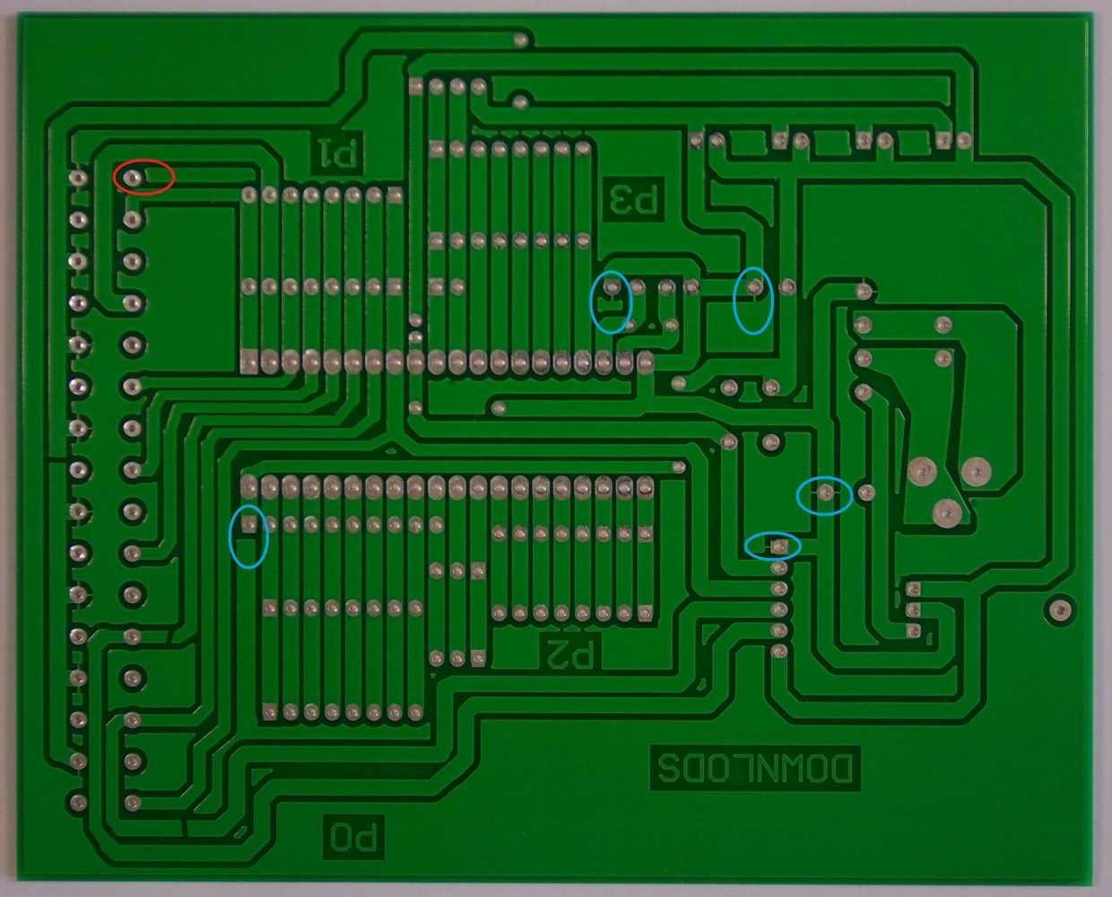
To reduce the number of defects on PCBs, a number of inspections are carried out at various points in the assembly line. With an increased number of PCB manufacturers and developers wanting a more compact and smaller circuit layout, companies have developed advanced inspection systems but still sometimes defects can go unnoticed. This project aims to look at three defects on a PCB and how machine learning can be used to identify them. One of the defects is missing holes which can be caused by faulty tooling or excessive processing. This hinders components or mountings to be put on the PCB. Next are the faulty defects: open and short circuits. These two can cause a device to be non-functional. An open circuit creates an infinitely high resistance therefore stopping current flow. A short circuit on the other hand creates a low resistance causing a high current to flow which can damage components or even cause a fire. While working on this project I built various models with MobileNetV2 SSD FPN-Lite 320x320, FOMO and YOLOv5 each with different parameters to achieve the best result. At the end, I settled on FOMO because it achieved a much better detection compared to the other models. Therefore to build our Machine Learning model, we will use FOMO and afterwards deploy the model to a Raspberry Pi 4B with the 8 megapixel V2.1 camera module.Quick Start
You can find the public project here: Manufactured PCBs Defects Detection. To add this project to your Edge Impulse projects, click “Clone” at the top of the window. Alternatively, to create a similar project, follow these steps after creating a new Edge Impulse project.Data Acquisition
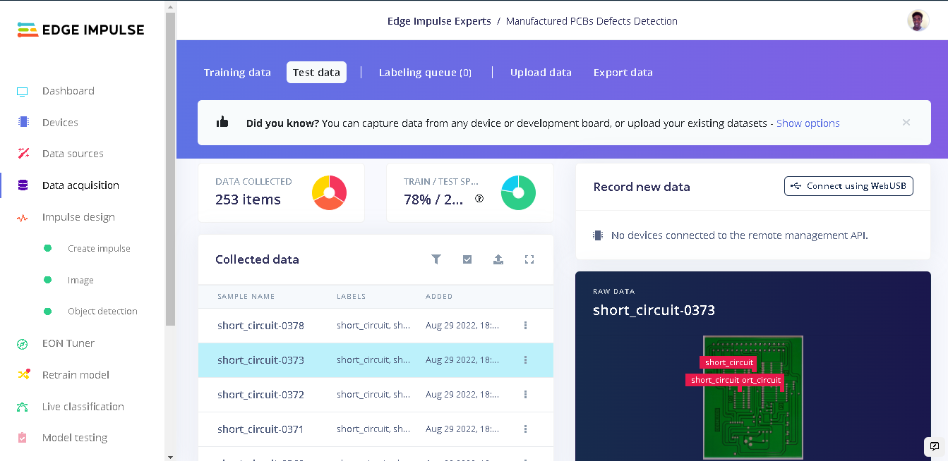
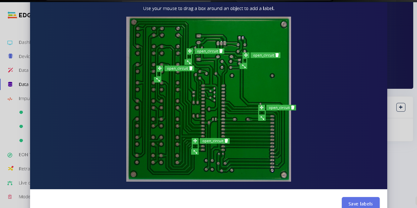
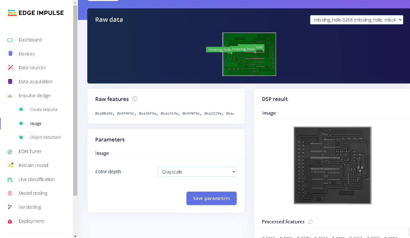
The dataset used in this project was sourced from Kaggle PCB Defects dataset. This dataset consists of 1366 PCB images with 6 kinds of defects. However for this demo, we will only use 3 kinds (missing hole, open circuit and short circuit) for our detection. This is because the annotations for this dataset are in XML format but the Edge Impulse Uploader requires a bounding_boxes.labels file with the bounding boxes in a unique JSON structure. For this project demo we will have to draw bounding boxes for all our images, therefore the need to reduce our dataset size. There are 9 PCBs used for this dataset. To create the dataset with the defects, artificial defects were added to the PCB images at various locations and saved as multiple images. These are high resolution images, which is a key factor in this object detection as lower resolution images reduce the useful information for object detection, which will in turn reduce the accuracy of a model. In total, we have 887 images for training and 253 images for testing. For each defect, we have a total of 380 images both for training and testing.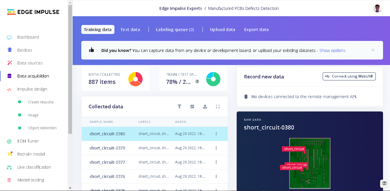
Impulse Design
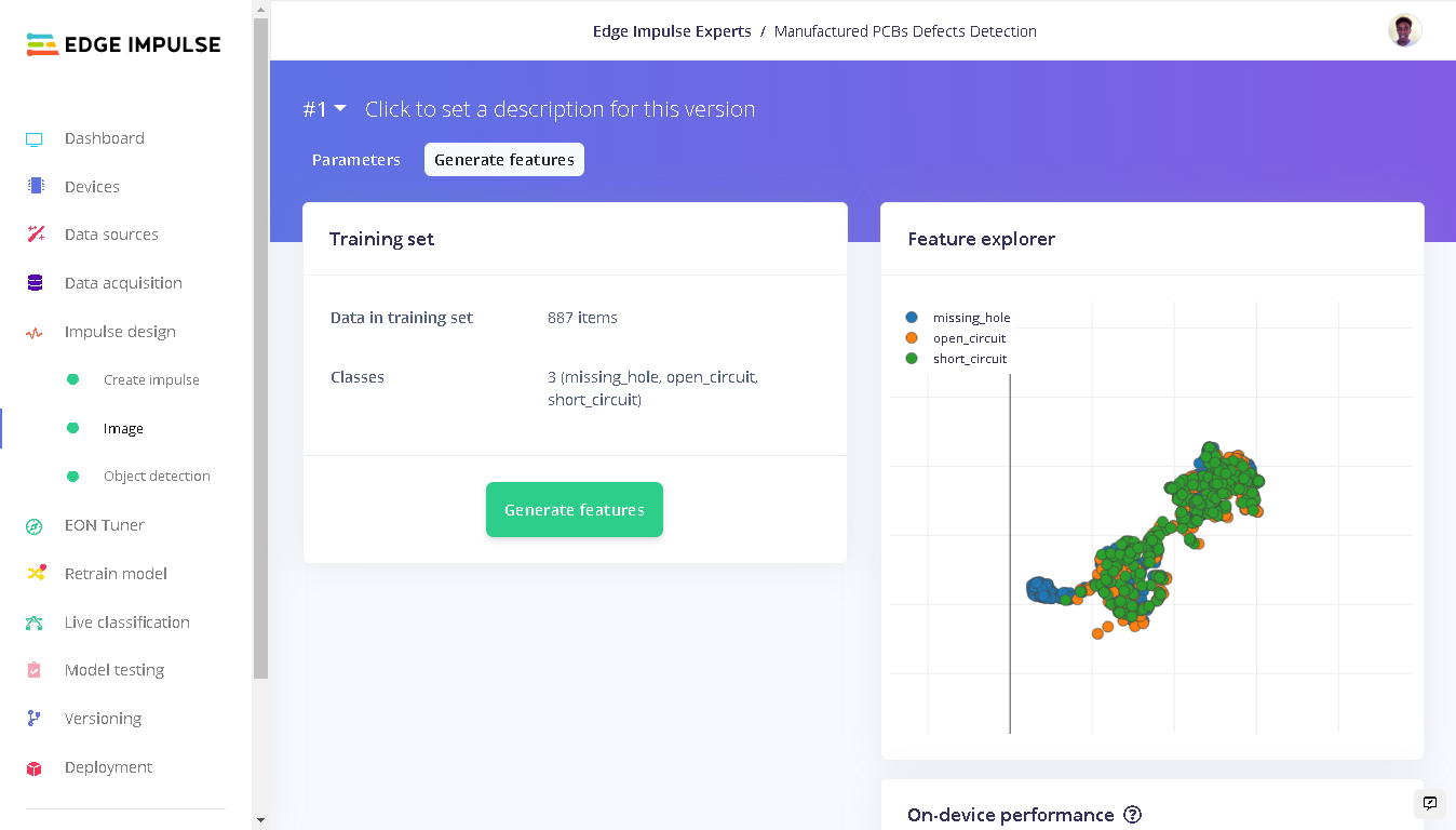
With our dataset in place we now need to configure important features: input, processing and learning blocks. This is a machine learning pipeline that indicates the type of input data, extracts features from the data, and finally a neural network that trains on the features from your data. Documentation on Impulse Design can be found here. We first click ”Create Impulse”. Here, set image width and height to 1024x1024 and Resize mode to Squash. Processing block is set to “Image” and the Learning block is “Object Detection (images)”. Click “Save Impulse” to use this configuration.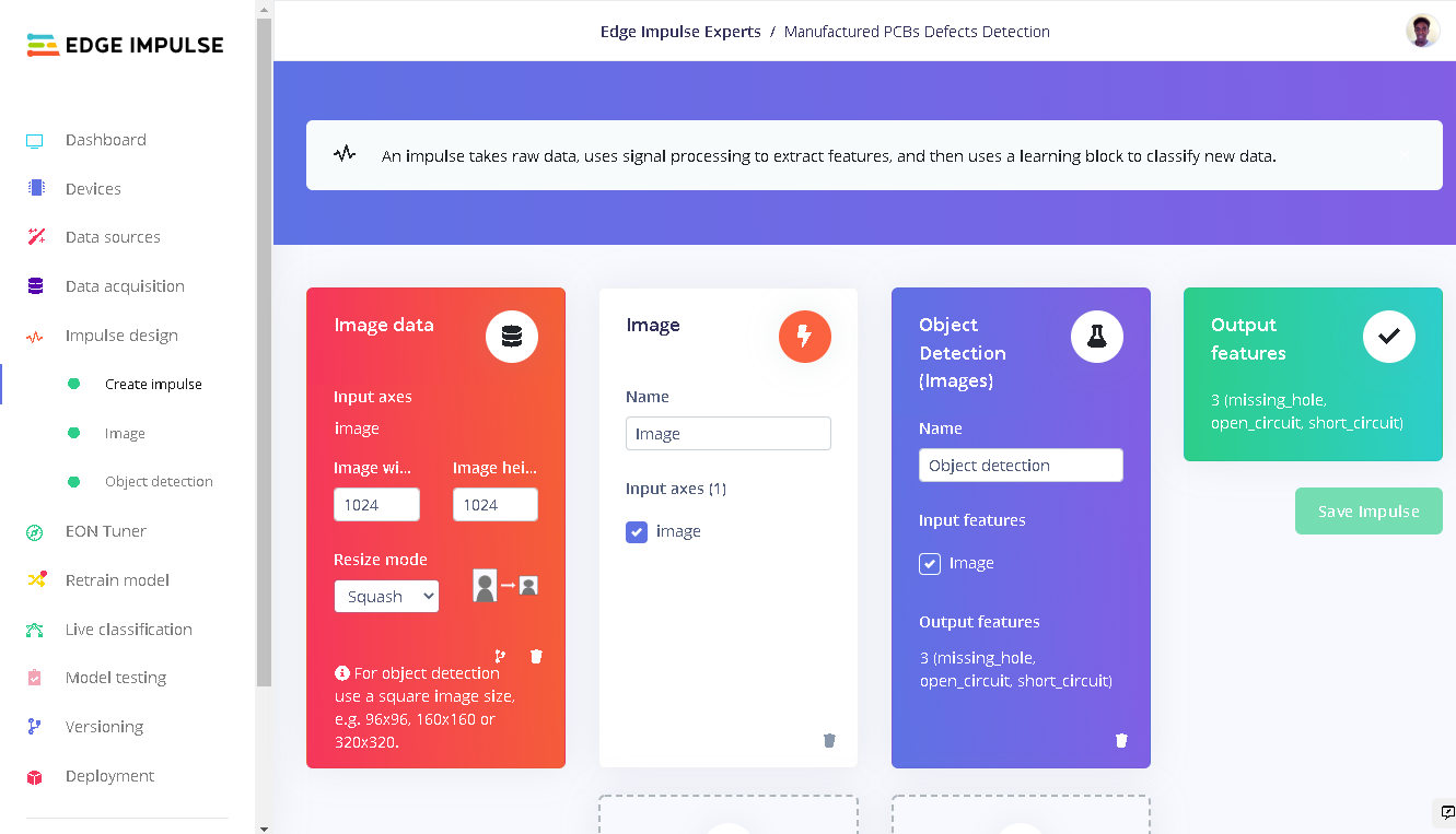
Discussion of the model performance - very interesting!
Training with FOMO (Faster Objects, More Objects) MobileNetV2 0.35
After training our model we get an F1 score of 48%. However, is an F1 score of 48% good or bad? This depends on the prediction (type of problem we want to solve).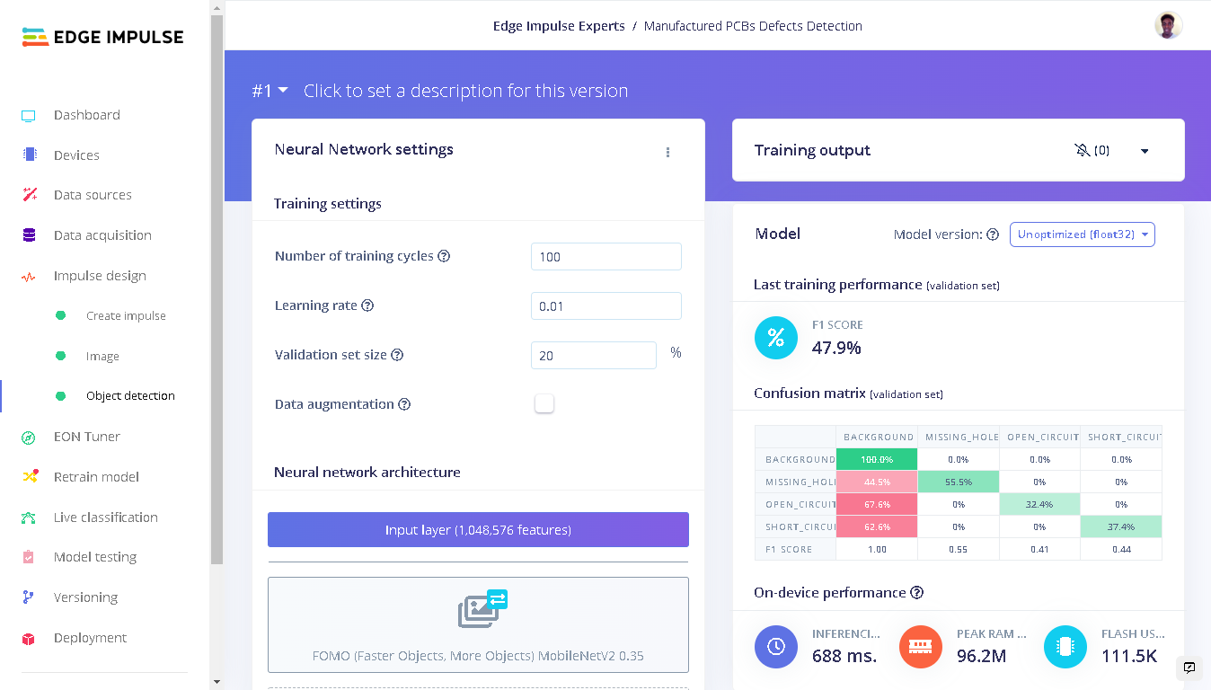

| Class | F1-score | Precision | Recall |
|---|---|---|---|
| missing hole | 0.55 | 0.54 | 0.56 |
| open circuit | 0.41 | 0.56 | 0.32 |
| short circuit | 0.44 | 0.54 | 0.37 |
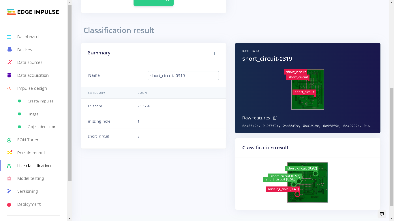
Model Testing
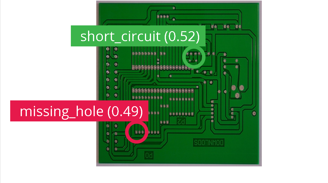
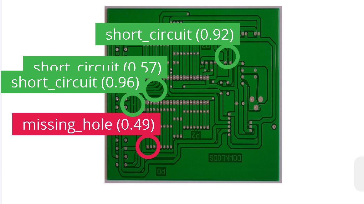
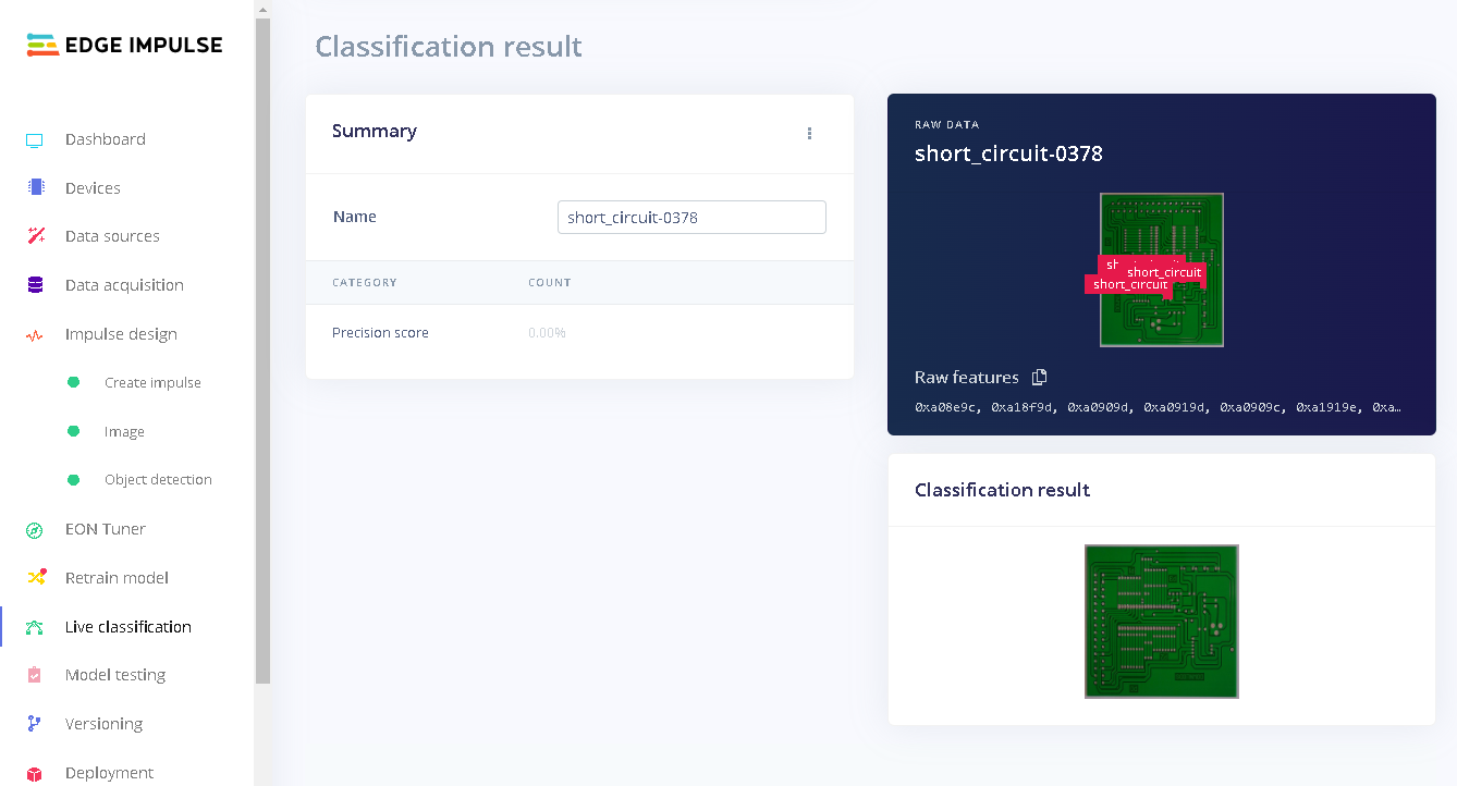
To test our model we go to “Model testing” and click “Classify all”. Our model has an accuracy of 13%, but wait! There’s more to this. Let’s discuss this result. Let’s look at the model performance for a test image that has an F1-score of 0%. This image has 3 short circuit labels and our model was able to accurately detect one short circuit in the PCB.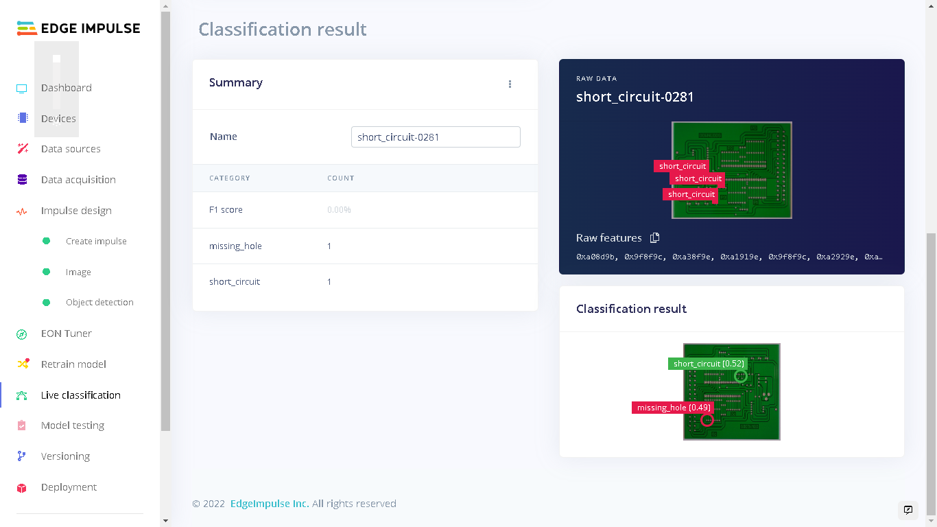
Training with YOLOv5
After training with FOMO and analyzing the results, I decided to train another model with YOLOv5 using the same dataset and classes. To train a YOLOv5 model on this custom dataset, I built a YOLOv5 model on my local computer using Edge Impulse custom learning blocks documentation and pushed it to my Edge Impulse account. This model was trained with various training cycles and learning rates. With 100 training cycles (epochs) and a learning rate of 0.01, The precision score of this model was not acceptable at 0.0%. FOMO has obviously performed much better compared to this model.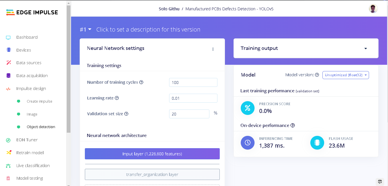
Deploying to a Raspberry Pi 4
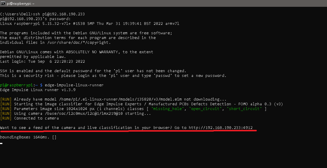
To deploy our model to the Raspberry Pi we first have to flash the Raspberry Pi OS image to an SD card, install Edge Impulse dependencies on the Raspberry Pi and connect a camera to the Pi. I used the 8 megapixel V2 camera module for capturing the images. Edge Impulse has documentation on how to setup the Raspberry Pi to connect to Edge Impulse studio and also deploying your model to the Pi. After setting up the Raspberry Pi, we can run the commandedge-impulse-linux to select our project from the Raspberry Pi then run the command edge-impulse-linux-runner to run our model.
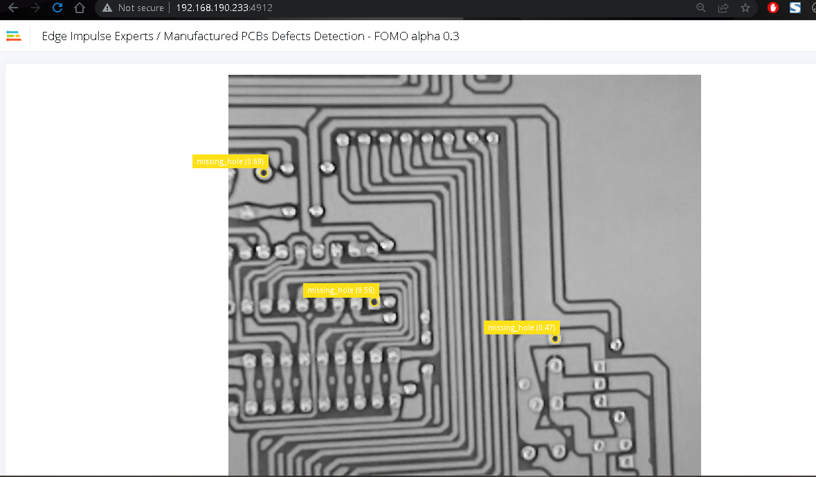
When running our model we can see live classification of what the Raspberry Pi camera captures and the inference. To do this, we connect a computer to the same network that the Raspberry Pi is connected to. Next, in a web browser we enter the url (likely an IP address) provided by the Raspberry Pi.